<?xml version="1.0" encoding="utf-8"?><feed xmlns="http://www.w3.org/2005/Atom" ><generator uri="https://jekyllrb.com/" version="3.10.0">Jekyll</generator><link href="https://dshu178.github.io/feed.xml" rel="self" type="application/atom+xml" /><link href="https://dshu178.github.io/" rel="alternate" type="text/html" /><updated>2026-04-25T23:15:26-07:00</updated><id>https://dshu178.github.io/feed.xml</id><title type="html">Dan Shu</title><subtitle>personal description</subtitle><author><name>Dan Shu</name><email>dshu178@gmail.com</email></author><entry><title type="html">MIMO-OFDM for 100G+/LANE Chip-to-Chip connection: SerDes, Highspeed I/O</title><link href="https://dshu178.github.io/posts/2023/08/blog-post-5/" rel="alternate" type="text/html" title="MIMO-OFDM for 100G+/LANE Chip-to-Chip connection: SerDes, Highspeed I/O" /><published>2023-08-19T00:00:00-07:00</published><updated>2023-08-19T00:00:00-07:00</updated><id>https://dshu178.github.io/posts/2023/08/blog-post-5</id><content type="html" xml:base="https://dshu178.github.io/posts/2023/08/blog-post-5/"><![CDATA[<h3 id="introduction-of-the-mimo-ofdm-based-highspeed-io">Introduction of the MIMO-OFDM based highspeed IO</h3>
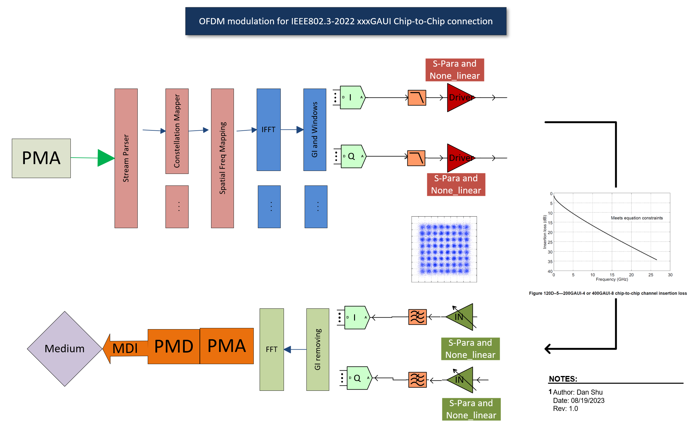
<p>With the ongoing increase in demand for higher System-on-Chip (SoC) I/O speeds, the significance of data rates for chip-to-chip (C2C) and chip-to-module (C2M) communication is becoming more crucial than ever. The adoption of PMA4 has become prevalent in SerDes design, and even the consideration of PAM8 modulation is on the horizon. However, while the relatively simple architecture of NRZ, PAM4, and PAM8 offers advantages, these modulation formats also suffer from suboptimal spectrum efficiency. This challenge is particularly pronounced when limitations in PCB or substrate RF bandwidth act as bottlenecks for achieving desired data throughput performance.</p>

<p><a href="/images/MIMO_OFDM-Modulation.png">
    <img src="/images/MIMO_OFDM-Modulation.png" />
</a>
<em>pic1 MIMO-OFDM for IEEE802.3 - 2022 xxxGAUI 100GBd+/LANE Chip-to-Chip connection</em></p>

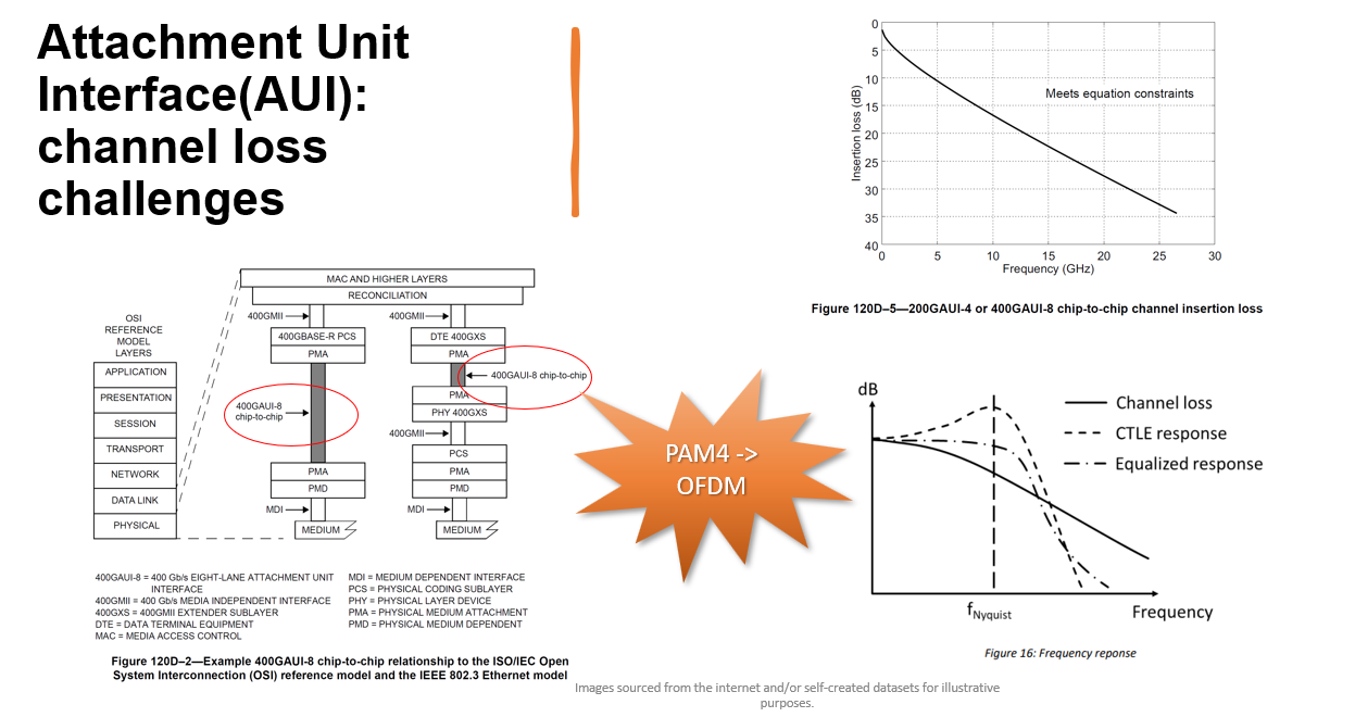
<p>Despite leveraging modern digital enhancements like Transmitter Finite Impulse Response (Tx FIR) and Receiver Continuous Time Linear Equalization (CTRL), Feed Forward Equalization (FFE), and Decision Feedback Equalization (DFE), we find ourselves confronted with the limitations of PCB/substrate bandwidth. These limits are evident when Insertion Loss (IL) reaches approximately -50 dB at frequencies around 80 GHz.</p>

<p>Existing solutions have explored doubling the overall data rate by doubling the total number of lanes. However, this approach is constrained by considerations such as silicon size, PCB dimensions, and the total number of I/O ports.</p>

<p>The upcoming era of high-speed I/O is poised to embrace the MIMO-OFDM architecture for SerDes. MIMO-OFDM brings forth a range of three key advantages when compared to NRZ, PAM4, and PAM8 modulation schemes.</p>

<p>1.  OFDM employs complex signals that exhibit double the spectrum efficiency when contrasted with real signals of NRZ, PAM4, and PAM8.</p>

<p>2.  MIMO demands reduced cross-lane isolation (8x8, 25dB) compared to PAM4’s requirement of &gt;40dB, leading to a more streamlined PCB RF routing design.</p>

<p>3.  The utilization of OFDM/QAM1024 results in a throughput that is 3.33 times higher than that achieved by PAM8, with a similar level of bandwidth and SDNR at 32dB.</p>

<h3 id="existing-highspeed-ioserdes-for-c2c-c2m-connection">Existing Highspeed IO/SerDes for C2C, C2M connection</h3>
<p>Below picture is the IEEE802.3-2022 attachment unit interface(AUI) to show the PCB insertion loss limitations.</p>

<p><a href="/images/IEEE802.3_AUI.png">
    <img src="/images/IEEE802.3_AUI.png" />
</a>
<em>pic2 Attachment Unit Interface(AUI): channel loss challenges</em></p>

<h3 id="complex-signal-over-real-signal">Complex Signal over Real Signal</h3>
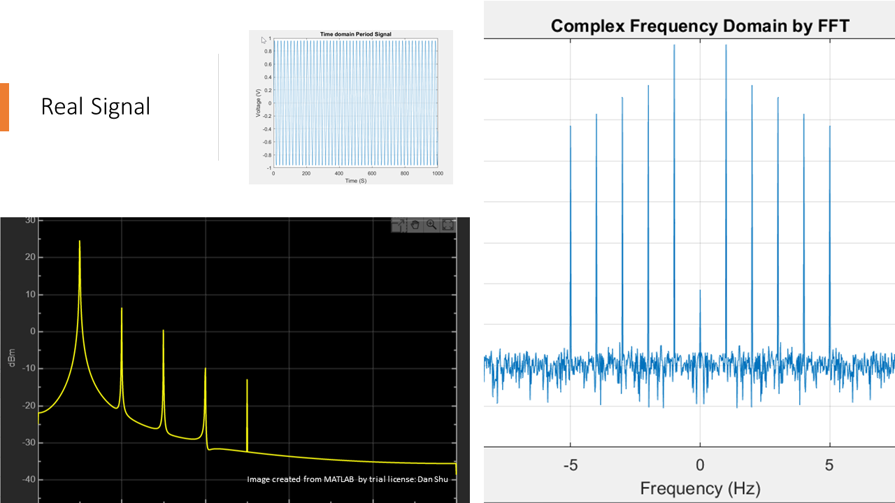
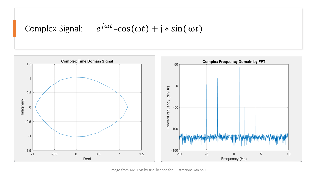
<p>Below pictures are the illustration of Complex Signal vs. Real Signal. A real signal is a type of signal that only contains real values. In other words, the signal values are real numbers, representing the amplitude or magnitude of the signal at a particular point in time. A complex signal, also known as a complex-valued signal, includes both real and imaginary components. The imaginary component represents a phase shift or angular information that complements the magnitude (real part) of the signal.
<a href="/images/Matlab_complex_signal1.png">
    <img src="/images/Matlab_complex_signal1.png" />
</a>
<em>pic3 The spectrum of a complex signal exhibits an asymmetric between negative and positive components.</em></p>

<p><a href="/images/Matlab_complex_signal2.png">
    <img src="/images/Matlab_complex_signal2.png" />
</a>
<em>pic4 Real signal</em></p>

<h3 id="example-considering-the-design-of-baseband-ofdm-for-bandwidths-of-10g20ghz40g80g">Example: Considering the design of Baseband OFDM for bandwidths of 10G/20GHz/40G/80G.</h3>

<p>Assume MII datarate=25Gb/s for NRZ and 25GBd/s for PAM4, the AUI one lane RF BW should be greater than 75%*25GHz= 18.75GHz. Let’s pick the 20GHz Baseband BW as the reference point to calculate.
1. I/Q requires 2 lanes if we use the NRZ/PAM4 AUI concept. The Complex signal BW is 40GHz. ADC/DAC clock rate will be 80~100GHz which is doable.
2. We employ 512 subcarriers with an FFT/IFFT size of 512 points. The subcarrier spacing will be 78.125MHz, and the symbol length, excluding the cyclic prefix (CP), will be 12.8ns.
3. Guard Interval (GI) for solving inter-symbol interference (ISI) issue in OFDM system. Three GI strategies we can consider: A. Cyclic prefix (CP) – commonly used in wireless industrial. B. Zero Padding – some coherent system. C. Zero-guard-interval for coherent system. Since GI is the overhead of throughput, smaller GI should be get faster lane speed. Our user case here is the PCB/substrate with length about 1mm~100mm. Even considering if we would use optical fiber CD/PMD model, the GI should be within 0.1ns.
4. Packet length. This could be a complex topic. Let’s assume MAC generate the package and Phy only rapacked it for sending. In this case, package length (how many symbols) will depending on Mac datasize, Phy’s FFT/IFFT engin power, and size of SRAM in SoC to do the calculation.</p>

<h3 id="at-end">At end</h3>

<p>The MIMO-OFDM SerDes design is poised to be compatible with PAM4 and has the potential to directly facilitate the driving of coherent optical MDI layer for simplifying the module design.</p>

<p>REFERENCES:</p>

<p>[1] <a href="https://standards.ieee.org/ieee/802.3/10422/">IEEE802.3-2022</a></p>

<p>[2] <a href="https://www.ieee802.org/3/B400G/public/21_05/lu_b400g_01_210517.pdf">Considerations on beyond 100G per lane electrical objectives: YuchunLU, Yan ZHUANG</a></p>

<p>[3] <a href="https://opg.optica.org/oe/fulltext.cfm?uri=oe-19-8-7451&amp;id=211579">Zero-guard-interval coherent optical OFDM with overlapped frequency-domain CD and PMD equalization: Chen Chen, Qunbi Zhuge, and David V. Plant</a></p>

<p>[4] <a href="https://dspillustrations.com/pages/posts/misc/the-cyclic-prefix-cp-in-ofdm.html">The Cyclic Prefix for OFDM</a></p>

<p>[5] <a href="https://citeseerx.ist.psu.edu/document?repid=rep1&amp;type=pdf&amp;doi=b9c70ed47c6857fab96ed12c937fc5495b235b6a">BER PERFORMANCE OF OFDM SYSTEM WITH CYCLIC PREFIX &amp; ZERO PADDING: Prafulla. D. Gawande and Sirddharth. A. Ladhake</a></p>

<p>========================</p>]]></content><author><name>Dan Shu</name><email>dshu178@gmail.com</email></author><category term="cool posts" /><category term="Architect" /><category term="Technology" /><category term="Sw tool" /><category term="IEEE802.3" /><category term="SerDes" /><summary type="html"><![CDATA[Introduction of the MIMO-OFDM based highspeed IO With the ongoing increase in demand for higher System-on-Chip (SoC) I/O speeds, the significance of data rates for chip-to-chip (C2C) and chip-to-module (C2M) communication is becoming more crucial than ever. The adoption of PMA4 has become prevalent in SerDes design, and even the consideration of PAM8 modulation is on the horizon. However, while the relatively simple architecture of NRZ, PAM4, and PAM8 offers advantages, these modulation formats also suffer from suboptimal spectrum efficiency. This challenge is particularly pronounced when limitations in PCB or substrate RF bandwidth act as bottlenecks for achieving desired data throughput performance.]]></summary></entry><entry><title type="html">RF Architect: Today, Tomorrow, and Future</title><link href="https://dshu178.github.io/posts/2023/04/blog-post-1/" rel="alternate" type="text/html" title="RF Architect: Today, Tomorrow, and Future" /><published>2023-04-03T00:00:00-07:00</published><updated>2023-04-03T00:00:00-07:00</updated><id>https://dshu178.github.io/posts/2023/04/blog-post-1</id><content type="html" xml:base="https://dshu178.github.io/posts/2023/04/blog-post-1/"><![CDATA[<p>As the demand for mobile data continues to grow, wireless devices are becoming more complex, requiring increased bandwidth and faster data rates. To address these challenges, a multi-carrier transmitter (Tx) architecture is emerging as a promising solution for future mobile wireless devices. This architecture allows for more power efficiency PA design, more efficient use of the available spectrum, enabling higher data rates and better signal quality. In this blog, we will introduce the multi-carrier Tx architecture and discuss its potential benefits for future wireless devices.</p>

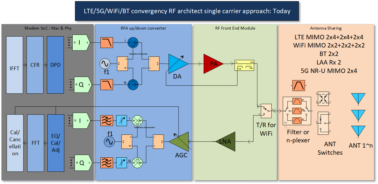
<p>1. Today’s designs only share a few designs among channels. Each RF signal has its dedicated hardware from lower layer PHY (PMD), including baseband, RFA, PA/LNA, filters, switches, and antennas, among others. When the total number of independent channels increases, the DC power consumption efficiency becomes low. Moreover, the complexity of PCB level tuning becomes much more difficult with an increasing number of RF chains.</p>

<p><a href="/images/Today_1v1.png">
    <img src="/images/Today_1v1.png" />
</a>
<em>pic1 Single Channel Tx/Rx example for today’s RF design</em></p>

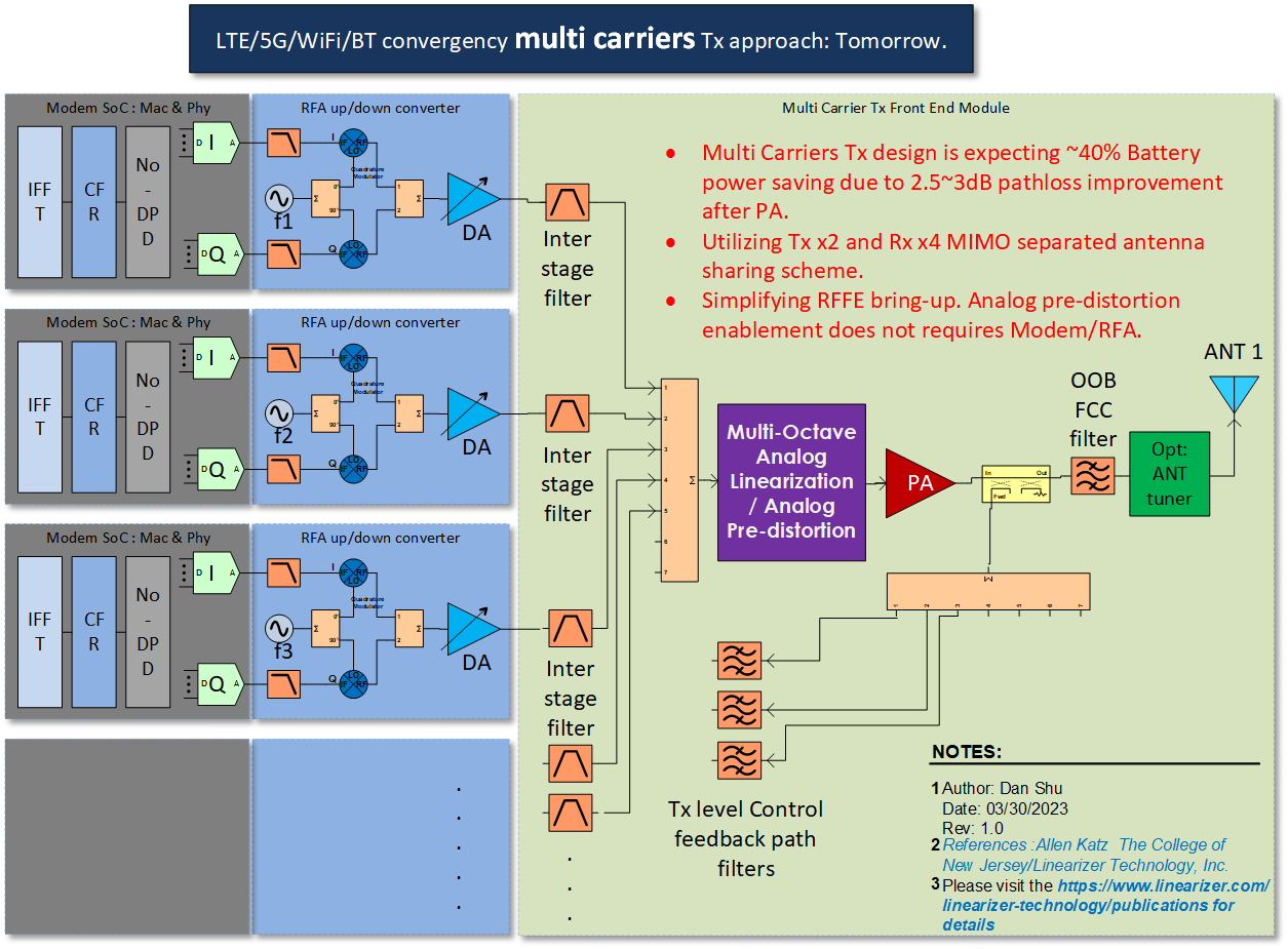
<p>2.  The Tx Architect of tomorrow aims to save approximately 40% of power consumption compared to today’s designs, resulting in a significant improvement in PCB level complexity and BOM cost. This improvement is mainly due to the removal of the post-PA complex RF switch/filter/n-plexer insertion loss (2.5~3dB).</p>

<p><a href="/images/Tomorrow_1v1.png">
    <img src="/images/Tomorrow_1v1.png" />
</a>
<em>pic2 Multi Channel Tx tomorrow’s RF design</em></p>

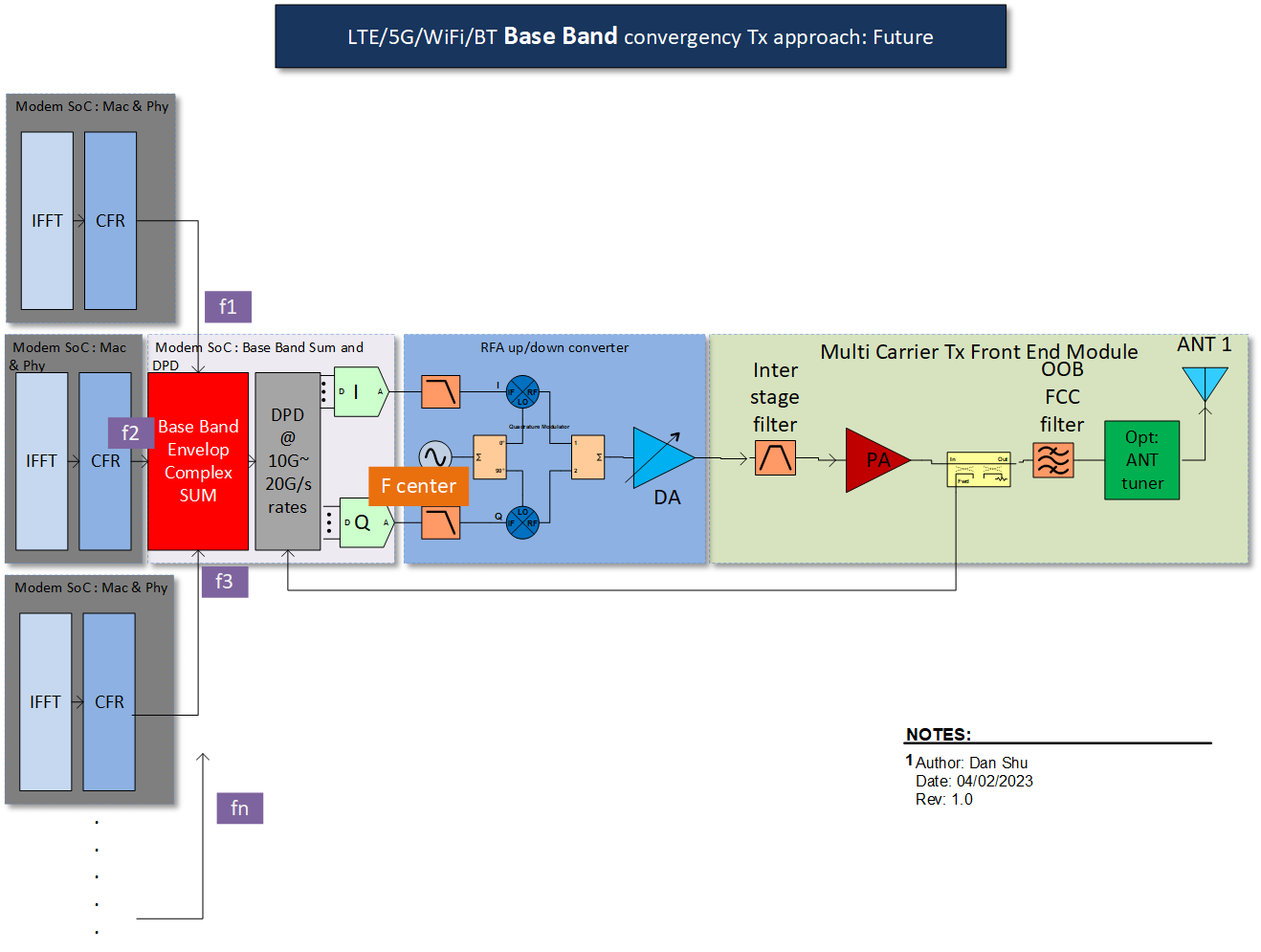
<p>3.  In the next 10 years, the Universal Tx Architect aims to sum the baseband (simulation of which can be done today on Matlab or SystemVue) of all the post-CFR data streams, after which the whole DPD function is applied to the combined baseband signal. This design will require a sample rate of 10-20G/s with 18-19 bits A-to-D conversion. Power consumption of the A-to-D converter at 10G/s needs to be reduced to the equivalent level of today’s 1G/s design.</p>

<p><a href="/images/Future_1v1.png">
    <img src="/images/Future_1v1.png" />
</a>
<em>pic3 Universal Tx Architect for future design</em></p>

<p>========================</p>]]></content><author><name>Dan Shu</name><email>dshu178@gmail.com</email></author><category term="cool posts" /><category term="Architect" /><category term="Technology" /><category term="Sw tool" /><summary type="html"><![CDATA[As the demand for mobile data continues to grow, wireless devices are becoming more complex, requiring increased bandwidth and faster data rates. To address these challenges, a multi-carrier transmitter (Tx) architecture is emerging as a promising solution for future mobile wireless devices. This architecture allows for more power efficiency PA design, more efficient use of the available spectrum, enabling higher data rates and better signal quality. In this blog, we will introduce the multi-carrier Tx architecture and discuss its potential benefits for future wireless devices.]]></summary></entry><entry><title type="html">Failed project: Digital negative delay in RF matching</title><link href="https://dshu178.github.io/posts/2023/03/blog-post-3/" rel="alternate" type="text/html" title="Failed project: Digital negative delay in RF matching" /><published>2023-03-15T00:00:00-07:00</published><updated>2023-03-15T00:00:00-07:00</updated><id>https://dshu178.github.io/posts/2023/03/blog-post-3</id><content type="html" xml:base="https://dshu178.github.io/posts/2023/03/blog-post-3/"><![CDATA[<p>Given that time is always measured positively, <a href="https://www.keysight.com/us/en/products/software/pathwave-design-software/pathwave-advanced-design-system.html">ADS</a> or other simulator can give a negative delay block in math. What does a negative delay in a circuit mean? A negative delay circuit/block could perfectly solve the wide band matching phase rotation issue.</p>

<p>Introduction. Negative delay could remove frequency-dependent wide band load-matching issues, and if achieved, the impact could be huge. However, in reality, L/C/line components all have positive delay. In the past, many of us have tried to use a network’s positive phase vs. frequency feature to achieve negative delay, but all attempts have failed with significant insertion loss.</p>

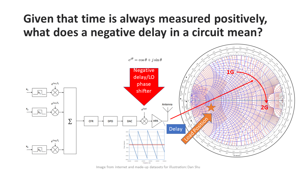
<p>1. What if we could achieve negative delay from a signal source using a digital approach, such as an FFT-based phase shift algorithm? I have tried a few ideas, but they all failed. The reason for my failure is that traditional FFT approaches can only manipulate I/Q amplitude and phase with voltage. However, the RF matching challenge lies in the fact that there is a phase shift between I and V due to impedance Z = R + jX. The reactance of Z shifts the V/I phase, which makes power delivery from point A to point B less efficient. In the worst case, 100% reflection could occur. So my first attempt at using an FFT approach to solve the matching issue failed.</p>

<p><a href="/images/Nagative_Delay1.png">
    <img src="/images/Nagative_Delay1.png" />
</a>
<em>pic1 Failed idea, digital pre-delay at LO/Mixer stage</em></p>

<p>2. The next step idea.</p>

<p><img src="/images/tobecontinue.png" /></p>

<p><em>pic2 thinking…</em></p>

<p>========================</p>]]></content><author><name>Dan Shu</name><email>dshu178@gmail.com</email></author><category term="cool posts" /><category term="Architect" /><category term="Technology" /><category term="RF" /><summary type="html"><![CDATA[Given that time is always measured positively, ADS or other simulator can give a negative delay block in math. What does a negative delay in a circuit mean? A negative delay circuit/block could perfectly solve the wide band matching phase rotation issue.]]></summary></entry></feed>